Simulation settings:
Sonnet box size is 100mm by 100mm.
The electrode is 10mm by 10mm.
The wiring from the electrode to the box wall is W=0.5mm and l=45mm.
The height of dielectric layers below and above the electrode is 50mm. Both of dielectric layers are air.
Analysis frequency is 10MHz, 1 point.
I put the Port 1 in the cross point of the wiring and the box wall. Here I observed the capacitance.
Fig. 1 is the 3D drawing of the geometry.
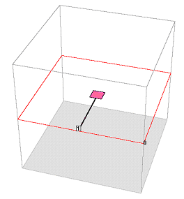
Fig. 1
After analysis I ran the response viewer--emgraph, which displayed the result, and set the display-settings to 'ZParams' and 'Magnitude' then I could see the impedance. |Z| was 20677 ohms. Applying the formula of Xc=1/(omega*C) I calculated that the capacitance was 0.770pF. This includes the capacitance of wiring.
Sonnet analyzes the inside of the metal box. The potential of the box is the GND level. We can suppose that this geometry has radial electric lines from the electrode to all the box wall like electric lines from a mono pole charge in the Fig. 2.
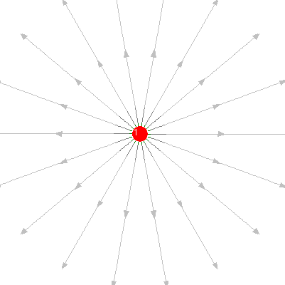
Fig. 2
Suppose that you reduce the size of Sonnet metal box. This makes the distance from the electrode to the box wall smaller. The capacitance will get bigger. Actually we have a capacitor between the box and the electrode.
You can make sure of it by making a simulation with a smaller box than my setting. For example, you can reduce the thickness of the layers.
Here we can suppose that capacitance of an electrode without a GND plane close is sensitive to close conductors. Then reproducibility of capacitance with this configuration is bad.
The settings of this case:
Sonnet box size is the same to the previous case. (100mm by 100mm)
The electrode is the same. (10mm by 10mm)
The wiring from the electrode to the box wall is the same. (W=0.5mm and l=45mm)
The height of dielectric layers below and above the electrode is the same (50mm). Both of dielectric layers are air.
Analysis frequency is 10MHz, 1 point.
I put a GND plane surrounding the electrode with 1.0mm clearance.
Fig. 3 is the 3D drawing of the geometry.
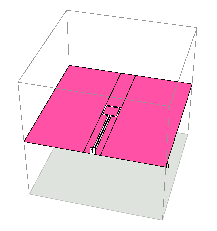
Fig. 3
Then I got |Z|=10874 ohms. The calculated capacitance was 1.46pF. This is the twice the previous case, Electrode without GND close.
The reason why the capacitance increases is getting the sensor electrode closer to a GND plane. In the previous case--2.1 the distance between the electrode and the GND is from the electrode to the box wall. In this case it got close to 1.0mm.
And we can suppose that electric lines gather in the gap between the electrode and the GND plane. We have few of electric lines to the box wall.
To make sure of it I had the height of the box short and made a simulation. (Fig. 4) The height of dielectric layers below and above the electrode was 5mm.
I got |Z|=10030 ohms. The calculated capacitance was 1.59pF. The variation by getting the ceiling and floor of the box close to the electrode is only +9%. Therefore we can suppose few of electric lines to the box wall.
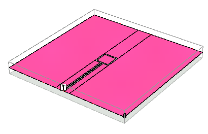
Fig. 4
Supposed using a t=1.6mm grass-epoxy FR-4 PCB, we have a GND plane on the backside.
The settings of the 3rd case:
Sonnet box size is reduced to 100mm by 35mm.
The electrode is the same. (10mm by 10mm)
The wiring from the electrode to the box wall is the same. (W=0.5mm and l=45mm)
The height of dielectric layers above the electrode is 90mm. The dielectric layers are air.
Analysis frequency is 10MHz, 1 point.
Fig. 5 is the 3D drawing of the geometry.
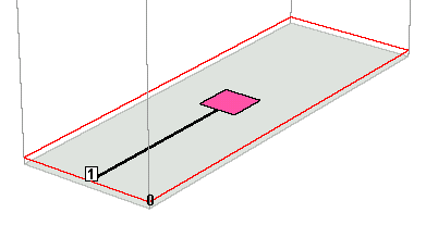
Fig. 5
Then I got |Z|=2592 ohms. The calculated capacitance was 6.14pF. This is 7 times as big as the case of Electrode without GND close.
It increases the capacitance very much to place a GND plane below an electrode. And electric lines gather in the gap between the electrode and the GND plane on the backside. It looks like a planar capacitor in an electromagnetics textbook. And we can also suppose fewer of electric lines to the box wall than case 2.2.
In this case I added a GND plane on the same layer to case 2.3. The clearance of the GND plane is the same to case 2.2.
Fig. 6 is the 3D drawing of the geometry.
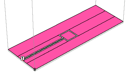
Fig. 6
Then I got |Z|=2474 ohms. The calculated capacitance was 6.43pF. The difference from Case 2.3 was only +0.29pF. That is, electric lines to the GND plane on the same layer just gave only 0.29pF. Therefore electric lines densely gather between the gap between the electrode and the backside GND plane. We can also suppose few of electric lines to others.
Summary
| Case |
2.1 |
2.2 |
2.3 |
2.4 |
| description |
Floating electrode |
Electrode surrounded with
a GND plane on the same layer |
Electrode on a GND plane
with t=1.6mm FR-4 PCB |
Electrode surrounded with
a GND plane on the same layer and on a GND plane with t=1.6mm FR-4 PCB |
| Capacitance |
0.770pF |
1.46pF |
6.14pF |
6.43pF |
In case 2.2 and 2.3, a capacitor is formed with a GND plane close to the electrode. It increases the capacitance of an electrode itself. In case 2.2 the capacitor is a line capacitor like a parallel wire or a twist-pair wire. In case 2.3 the capacitor is a planar capacitor.
Line is the 1st dimension. Plane is the 2nd dimension. You know, a plane increases capacitance more than a line, by square rate.
|
Type of capacitor |
Influence |
Example |
| Case 2.2 |
Line capacitor |
1st dimension |
Pararell wire |
| Case 2.3 |
Planar capacitor |
2nd dimsnsion |
Capacitor component |
| Case 2.4 |
Line capacitor
& Planar capacitor |
2nd dimsnsion >>1st dimension |
|
(C)KANAYA Hidenori
Hide's Radio Shack


